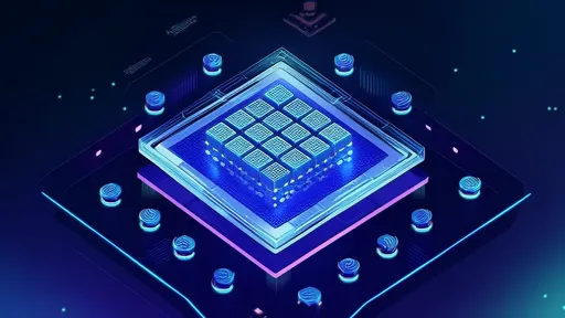
The semiconductor industry stands at the precipice of a transformative era as researchers explore alternatives to silicon-based transistors. Among the most promising candidates is phosphorene, a two-dimensional (2D) material derived from black phosphorus. With its unique electronic properties and potential for high-performance switching, phosphorene transistors are emerging as a viable successor to traditional silicon devices, offering solutions to the limitations of Moore's Law.
Phosphorene: A Rising Star in 2D Materials
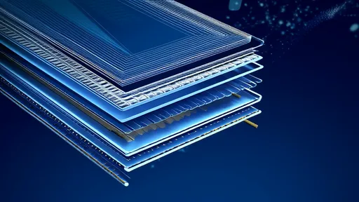
Unlike graphene, which lacks a natural bandgap, phosphorene possesses a tunable direct bandgap that makes it exceptionally well-suited for transistor applications. This property allows it to efficiently switch between conducting and insulating states, a critical requirement for digital logic circuits. The anisotropic nature of phosphorene—where its electronic and thermal properties vary along different crystal directions—further enhances its appeal for designing specialized electronic devices.
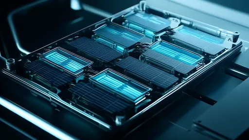
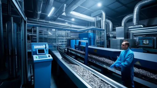
Recent advancements in fabrication techniques have enabled the production of high-quality phosphorene layers, though challenges remain in achieving large-scale uniformity. Exfoliation methods, similar to those used for graphene, have proven effective in laboratory settings. However, researchers are now focusing on chemical vapor deposition (CVD) and other scalable approaches to make phosphorene commercially viable.
Performance Advantages Over Silicon
Phosphorene transistors demonstrate several key advantages over their silicon counterparts. Their ultra-thin structure allows for superior electrostatic control, reducing short-channel effects that plague modern silicon transistors as they shrink to nanometer scales. Experimental devices have shown impressive carrier mobility—exceeding 1,000 cm²/Vs at room temperature—which translates to faster switching speeds and lower power consumption.
Perhaps most significantly, phosphorene maintains its excellent electronic properties even when scaled down to atomic thicknesses, a feat that silicon struggles to achieve. This characteristic positions phosphorene as an ideal material for future generations of ultra-dense integrated circuits. Additionally, its inherent flexibility opens possibilities for flexible electronics and wearable applications where silicon's rigidity becomes a limitation.
Challenges and Stability Concerns
Despite its promise, phosphorene faces notable hurdles before it can challenge silicon's dominance. Environmental stability remains a primary concern, as phosphorene degrades when exposed to oxygen and moisture. Researchers are actively developing encapsulation techniques using materials like aluminum oxide or hexagonal boron nitride to protect phosphorene devices from atmospheric degradation.
Another challenge lies in contact resistance between phosphorene and metal electrodes. The formation of clean, low-resistance contacts is crucial for optimal transistor performance. Recent studies have shown that careful selection of contact metals and interface engineering can significantly improve charge injection efficiency, bringing phosphorene transistors closer to practical implementation.
Integration with Existing Semiconductor Technology
The semiconductor industry has invested trillions in silicon infrastructure, making complete replacement unlikely in the near term. Instead, researchers envision hybrid approaches where phosphorene complements silicon technology. One promising direction involves using phosphorene transistors for specific functions where they outperform silicon, such as in high-frequency applications or ultra-low-power circuits.
3D integration represents another potential pathway, with phosphorene devices stacked atop conventional silicon chips. This approach could leverage the strengths of both materials while maintaining compatibility with existing manufacturing processes. Several research groups have already demonstrated functional hybrid circuits combining silicon CMOS with 2D materials, including phosphorene.
The Road to Commercialization
While laboratory prototypes show great promise, significant work remains to bring phosphorene transistors to market. Reliability testing under various operating conditions must be conducted, and manufacturing processes need refinement to achieve high yields. Industry analysts predict that if these challenges can be overcome, we might see initial phosphorene-based products within the next decade, likely in specialized applications where its unique properties provide clear advantages.
Investment in phosphorene research has been growing steadily, with both academic institutions and semiconductor giants exploring its potential. Patent filings related to phosphorene devices have increased dramatically in recent years, signaling industry interest in this emerging technology. As the limitations of silicon become more pronounced, the push for alternative materials like phosphorene will only intensify.
Future Prospects and Research Directions
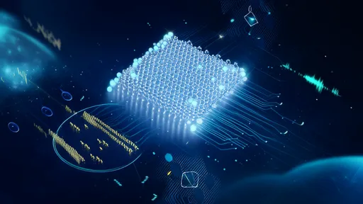
Looking ahead, researchers are investigating ways to further enhance phosphorene's properties through strain engineering, chemical functionalization, and heterostructure formation with other 2D materials. These approaches could unlock new functionalities and improve device performance beyond what pure phosphorene can achieve.
The development of phosphorene transistors also drives progress in related areas such as photonics and sensor technology. The material's strong light-matter interaction makes it attractive for optoelectronic applications, while its sensitivity to surface adsorbates suggests potential in chemical and biological sensing.
As the scientific community continues to unravel phosphorene's capabilities, one thing becomes increasingly clear: this 2D material represents more than just another semiconductor—it embodies a potential paradigm shift in electronics that could redefine computing power efficiency and open doors to entirely new applications beyond the reach of silicon technology.
By /Jul 28, 2025
By /Jul 28, 2025

By /Jul 28, 2025

By /Jul 28, 2025

By /Jul 28, 2025

By /Jul 28, 2025
By /Jul 28, 2025

By /Jul 18, 2025

By /Jul 28, 2025

By /Jul 28, 2025

By /Jul 28, 2025

By /Jul 28, 2025
By /Jul 28, 2025

By /Jul 28, 2025
By /Jul 28, 2025

By /Jul 28, 2025
By /Jul 28, 2025
By /Jul 28, 2025

By /Jul 28, 2025
By /Jul 28, 2025